Not much public work to show, mostly investigating potential manufacturing partners.
Farnell order is dribbling in, my PCBs and AliExpress orders have been shipped. All the pieces should be ready when I get back next week.
Play
Went to Canberra on Friday to catch up with folk and party, staying for the week.
Discovered Coconuts Duo amazingly fun to play and spectate. It’s probably even fun sober.
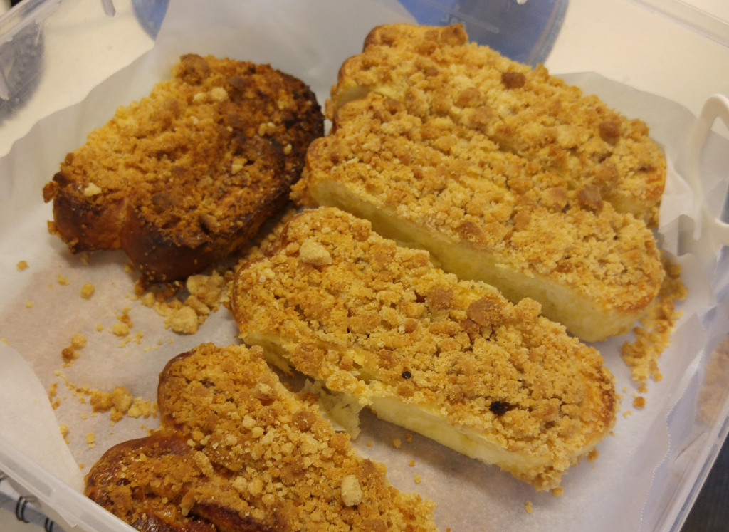
Made marbled butter biscuits (pictured). Annoyingly fragile to being burnt but fortunately I made so many that after chucking 15% I still needed two containers to store them all.
One of the key features of my microwave is Panasonic’s Grideye thermal sensor. This is a (relatively) low cost thermal sensor that I have placed at the top of the microwave to measure the surface temperature of the food.
The sensor is an I2C device which requires a 5V or 3.3V supply. Wanting to keep everything relatively high level I am implementing it as a USB device.
For the demo I used a BusPirate as an I2C-USB bridge. This got me through the demo but the protocols combine very badly resulting in a maximum frame rate of about 1fps. The high latency of USB communications combines with the chattyness of I2C causing everything to be very slow. So a practical implementation can’t be a bridge, it must have some logic to control the device and present a processed USB data stream.
There is an existing one, Digikey has a breakout board that their Application Engineers developed. Sadly due to Panasonic’s limitations on distributing the GridEye sensor they only ship them within the US. The Application Engineers team runs in an open hardware manner, the project page for the breakout board includes the circuit diagram and firmware code. I got in contact with the author, Chris Baird, and while he didn’t have any blank PCBs he could ship he was happy to share the gerber files so I could make my own.
The story doesn’t end here though, because a solid dose of Not-Invented-Here hit, justified by the twin desire to evaluate KiCad and wanting to implement the USB Video protocol, driven in part by an absurd desire to shovel yet another driver into the Linux Kernel.
As a nice bonus I reduced the cost, significant components, excluding the GridEye, cost $9.81 AUD for the Digikey board compared to $2.60 AUD for mine. Though that it no way compensates for the time spent and comes with the disclaimer that the Digikey board actually works.
My circuit design is below, I took a rather different approach to the Digikey board, wiring an Atmel AVR directly to the USB input. This will use V-USB, a software USB stack to communicate. The ATTiny AVR used is capable of running V-USB on it’s internal crystal, it should also have enough memory allowing me to do USB based reprogramming.
The AVR must run off 5V in order to be fast enough to handle the USB communications. USB communications however are a 3.3V signal and while driving it at 5V typically works it’s certainly not a nice thing to do. The weak zenner diodes are a bidirectional level conversion technique.
The power network actually allows for two different voltage levels into the GridEye. It isn’t clear from the datasheet what impact a dirty power supply has, so I have fitted an LDO to create a smooth 3.3V signal. There is also a 5V GridEye variant (which I don’t currently have) that could be run directly off the USB rail. To support both cases I have an LDO designed in as well as pads for a zero ohm resistor to bridge the rails, one or the other should be fitted.
The I2C bus uses an open-collector signal so nicely adapts to whatever voltage the GridEye is powered on. Running at 5V the AVR reads 2.5V as high, comfortably supporting 3.3V communication.
I would have liked to have a spare IO to be able to disable the LDO in low power mode. However the GridEye can be software configured into a low power state and the LDO does not consume much power when idle. I could repurpose the reset line for the job but that has significant downsides.
Single Sided PCB
Click image for interactive 3D model
Loading …
My first attempt at a PCB was a two layered single sided PCB, it is functional but not optimized as I decided the approach was wrong and created a double sided PCB for manufacturing.
It is a fairly long, simple, PCB with a simple flow left to right of the USB port, AVR chip and GridEye sensor.
I created two ground planes, a shield plane around the outside which is connected to the USB shield and the screw holes, it is designed to be connected to the chassis. The center of the board has a standard digital ground connected to various components and the USB ground line. In my microwave system there should be a central (star) ground point, somewhere else, which connects these two grounds. To provide flexibility, mainly for applications without a metal chassis, there is an empty 0603 pad in each corner to bridge the two ground planes with either a capacitor or a 0 ohm resistor .
After doing this layout I felt a two layer design would be much better. It would allow the board to be much smaller and I wanted the sensor to be more central. Later I learnt that the prototype PCB manufacturers all up their rates for boards over 5cm, so my 6cm board was fairly expensive. I swapped the large six pin connector with a Tag-Connect connector to try and be less ugly, with mixed success.
Two Sided PCB
Click image for interactive 3D model
Loading …
I started this board more professionally, defining a 3cm by 2cm board with M2 holes on each corner. It was a little bit of a struggle to get everything to fit nicely but that probably means it was the correct size.
My main concern with the new design is that one of the USB data lines is also used in the programming process. I tried to make it as short as possible but the programming connector wouldn’t fit anywhere but the far side of the board to the USB connector. So that line is a long stub during operation, not a nice thing to do to an RF signal. Anecdotal evidence from forums suggests that I will get away with this but having the programming cable connected will cause it to fail, I’m happy with that.
The Tag-Connect connector can be seen on the far side to the USB port. It is actually just a carefully arranged collection of pads with holes to guide the plug. I haven’t used the Tag-Connect system before, I am attracted to it for a number of reasons. The footprint is smaller, in board size, only consuming one layer and not having a high part permanently attached. Being a layout of pads it is cheap per board. And for manufacturing it is easy to design a pogo pin setup to hit the pads or use a bed of nails system. There is also a series of test points exposing the USB lines for manufacturing.
Several people have complained about the Tag-Connect routing meaning that you take up as much board space as the standard, larger, connector. I certainly found the routing was annoying, especially with the holes at either end requiring lines to go the long way around. I cheated somewhat by placing vias on the pads, effectively making some of the pins through holes, this made routing much easier for me. For a two layered board the Tag-Connect benefits are probably marginal, with more layers the benefits would be add up rapidly.
Ordering
An order has been placed at OSHPark for both the Digikey board and mine, the process was remarkably good, lots of feedback as to what would be manufactured as you progressed. My board has an oval hole which OSHPark doesn’t support but I’ll fix that somehow after the board is delivered.
The Digikey board 20.35×22.91 mm (0.8×0.9 inches) and cost $1.20 USD per board.
My board is 30.02×20.02 mm (the 0.02mm is the cut line thickness) and cost $1.55 USD per board.
Within 24 hours both boards had been sent for fabrication, mine got a free upgrade to the special rush order stream.
I have ordered an 0603 resistor and an 0603 capacitor part book from Super Deal Technology with some empty pages. The Digikey board uses 0804 parts (designed for old folks with fading eyesight) but I’ll just put 0603s onto the larger pads. Part books are by far the best way to manage SMD components.
The remaining parts have been ordered from Element14, Digikey was cheaper on the parts but more expensive with shipping.
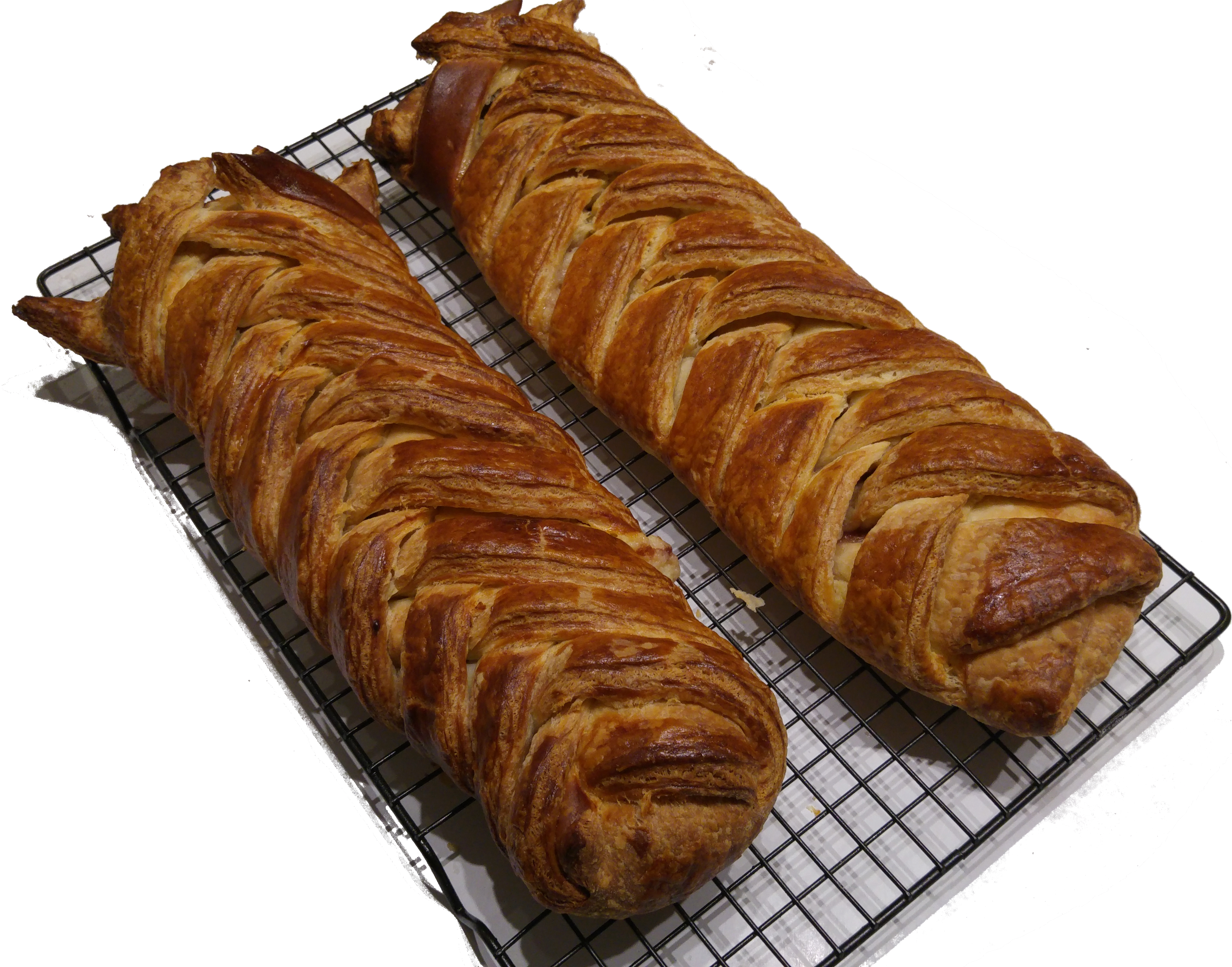
Baked my first successful Danish using an online recipe after two failed attempts following a recipe book. We ate one and gave one away to my Grandfather.
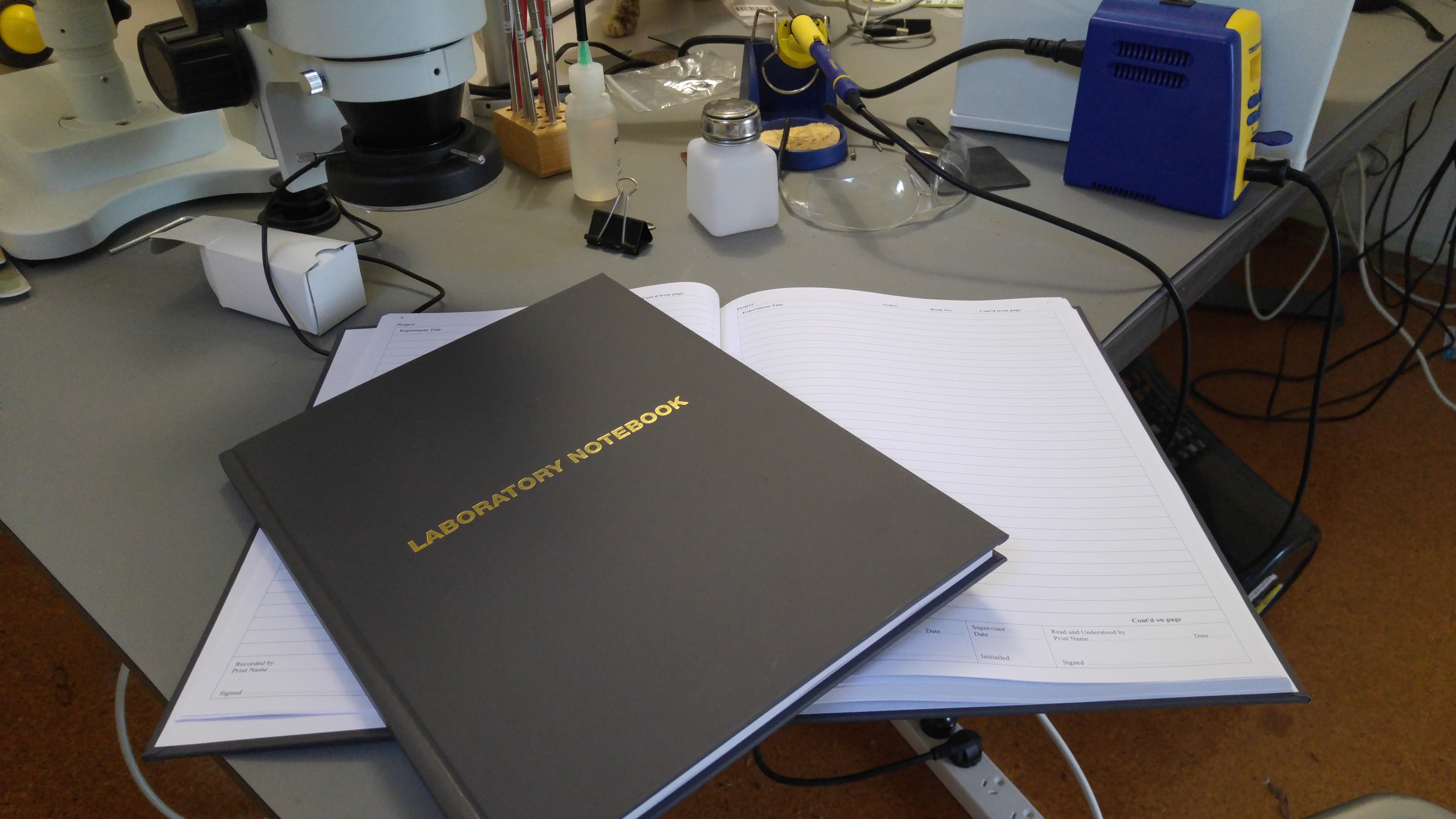
Had my new engineering notebooks delivered, official CSIRO stock. I had a terrible time trying to find a decent book, my current one is an art book I picked up from OfficeWorks and it wasn’t ideal. The current book has a few pages left, I’ll probably transition over to a new one in a week or two.
I have been experimenting this week with circuit design and pcb layout tools. My experience is with Altium
but the price is rather hefty for my fairly simple requirements and
while I have used Altium for a few years I never actually liked it,
there are a lot of issues with the system. I considered thevariousonlinetools and Eagle before deciding to give KiCad a go.
KiCad
is an open source bundle of tools which has been rapidly increasing in
quality over the last few years. CERN is providing professional
development support and they have recently transferred from a ‘build the
source’ release structure to standard point releases.
I have played with KiCad for most of the week. It is good, I could do everything I needed to for the basic board I was doing, but some of it was a struggle. There are a lot of rough edges, however the community seems strong and most of the issues I encountered are in the process of being fixed.
There are several projects under the KiCad banner which loosely
interoperate, it seems they have had varying amounts of coordination
over the years. Kicad itself is a project manager and application
laucher. Eeschema is the schematic design software. Pcbnew does the PCB
layout. There are other tools I haven’t played with yet, such as a
gerber viewer.
One of the issues is the cooperation between these applications. For
example the controls such as keyboard shortcuts and mouse behaviour are
inconsistent (This is flagged to be fixed by introducing a global
shortcut manager 🔗.
For a while (since fixed) pcbnew had panelization features available
when launched standalone but not when launched from within kicad 🔗. These sort of problems mean that it feels more like using several different programs than a unified suite.
Breaking news
I have published a writeup of the board I designed, at /grideye-usb/.
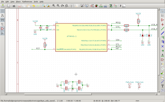
Eeschema
Eeschema screenshot
Eeschema is nice and familiar, you can place parts, connect wires,
create named nets etc. I had a very simple five component board so had
no need of the advanced features. However there was obvious
functionality for buses and a fair bit of support for nested sheets.
There is annotation tool to name your parts and a basic rule checker to
catch mistakes.
Bonus
A nice bonus for Eeschema is the ability to have two names on a net.
This is a bit controversial, Altium forbids it but I like it. Some times
a line has two roles, such as being the MISO communication line during
programming and the I2C interrupt line during normal operation. I like
being able to create a named net for each role and connect both to the
pin of the chip. The PCB layout program needs a single name, Eeschema
handles this by arbitrarily picking one of them.
Missing Feature
Altium has a feature they call directives.
This allows a pair of wires to be identified to be routed as a
differential pair. You can also specify net classes, so as to specify
increased track widths for the power rail or the required clearance on a
high voltage track. KiCad does allow this to be done in Pcbnew but I
feel the schematic, as the documentation for the design, should contain
this information. This is particularly important if the layout and
design are performed by different people.
Awkward
Eeschema’s use of dragging with the left mouse button is odd. In most
applications this would perform a group select, in eeschema it selects
and begins to move the components. Copy/paste is done by holding down
shift before doing a selection. The oddness and learning curve aside,
this doesn’t scale well. There is no way of selecting a group of objects
so you can’t do a group delete, you can’t change the properties of a
group or resize multiple wires together. Using the copy/paste you can’t
double check what you have selected before doing a copy, multiple pastes
require the full process to be run again and you can’t change sheets.
The move is still the action regardless of the tool selected, so
dragging with the wire tool actually does a select/move and placing a
box like a sub-sheet must be done with two clicks not a drag.
I suspect the select behaviour will be changed in the same batch of work as the shortcut improvements. 🔗
Ugly
I should open by saying I couldn’t really get my head around the
schematic libraries. My understanding is that a library file can hold
multiple components but I couldn’t figure out how to put a second
component into a library file. I did see notes suggesting that you merge
two libraries by editing them by hand.
Several people have created their own tools to try and assist managing libraries 🔗🔗🔗. The existence of these tools indicates that many others have also encountered problems.
There is hidden magic behind the library process. For example to
create a power component, basically a power net flag, the pin must be
hidden. The pin still gets a wire connected to it but if it is not
hidden it doesn’t connect to the power net and you get unconnected
errors when running the rule check. This isn’t documented, the nice
folks in the IRC channel explained it to me.
There is also documented hidden magic where some parts, fortunately
none I used, have hidden VCC pins so they magically get the power rail
without cluttering your schematic. Which is not so useful in the modern
environment of multiple signal levels.
The developers are well aware of all of these issues, half the roadmap entries for eeschema are related to component editing. 🔗
The plan seems to be to migrate the backend of the schematic library to
the pcb library file format and work. Then build better editing tools
on top. The PCB library tool is a significant step forward.
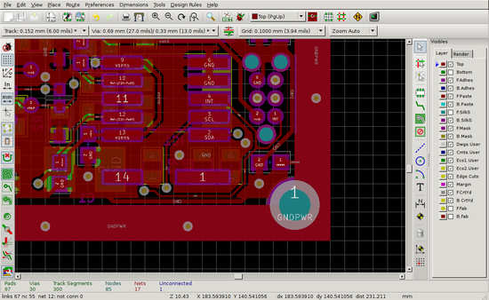
Pcbnew
Pcbnew screenshot
It took me a while to realise that there are actually three different
PCB programs bundled into Pcbnew. They are listed in the view menu as
three different display modes: default, OpenGL, and Cairo. This is not,
as you might expect, just a different display engine. Some features are
not available in all modes and some features work differently depending
which mode you are in. I found Cairo ran very slowly on my poor ancient
laptop so I just used default and OpenGL.
Differential routing is a relatively new feature and is only
implemented in OpenGL. In the default view the feature on the menu is
simply disabled, grayed out, no feedback is provided as to how to enable
it. 🔗
There are other, lesser issues:
In GL mode the scroll bar arrows don’t work, dragging does.
Rubber band drag mode only works in default mode.
In normal mode deleting a track deletes the attached via, in GL mode it does not.
In normal mode the start track shortcut starts a track immediately, in GL mode it waits for a click.
There is a 3D model feature which uses VRML world files for each part. However it only supports the subset generated by wings3d, more complex files silently fail. Extending this to other model types is on the roadmap.
Some other stuff feels a bit incomplete:
Hiding a copper layer still shows the pads.
There is a “Hide all copper layers but active” option for single sided work but it doesn’t hide the other side’s silkscreen.
The rule-check doesn’t enforce track width.
Finally the library management is better than Eescheema’s but still needs a lot of work.
Relative paths require manually using an environment variable, which
was listed in the Eeschema library manager but not Pcbnew’s.
There is a plugin to add github based repositories, but the option is listed even if the plugin is not installed.
There is a plugin to add github based repositories, not git based, it uses a github webpage URL.
Adding a library doesn’t check that the library exists, works or is valid. An error is shown later when you try and use it.
A few weeks ago I did a talk on my Microwave project at linux.conf.au it took me a while to be brave enough to watch myself and it wasn’t as bad as I thought. The talk was certainly well received, the feedback was positive and useful, there were about 150 people in the room and the youtube copy has clocked almost 400 views so far. I also got a writeup published by Linux Weekly News.
There is a lot I am taking away from the process, I don’t think I have been so unprepared in my life but managed to get away with it. The response from people was far more favourable than I expected, in particular I was surprised that most of the questions have engaged at the concept level rather than the implementation details. A few people commented that they saw me settle and become less nervous a short way into the talk, in reality I realised I was blowing through the material far too quickly and just tried to slow down, I think I did settle a bit once the questions started flowing though. I also did not understand the realities of a large group practising passive listening, for example people listening while playing with their laptop or phone, rather disconcerting when you look up and feel that nobody is paying attention.
Feedback
Some interesting feedback was people seeing possibilities to use the microwave for things that microwaves are not customarily used for, I confess I had been blind to this. In particular tempering chocolate and sous-vide cooking both require holding the temperature to set level for a prolonged period. Other precise heating processes like heating sugar are also interesting options.
Several people suggested just doing the electronic work and abandoning or delaying the mechanical modifications until the next model. This was something I looked at early on and decided against but the arguments are certainly strong enough that I will be reconsidering it.
At the end of the talk I conducted a price point survey which showed that many people felt the product was worth $500 AUD but baulked and $1000 AUD. Which doesn’t mean that I wouldn’t find sales at the higher level but life is easier closer to $500. These prices include compensation for the increased risk of the kickstarter process.
Discussions on eevblog raised that solid state microwaves are coming. I thought that they would be about ten years out but it looks like it will probably be two to three years, manufacturers are advertising that commercial units will be available at the end of the year. This is interesting and sets a time limit to the project but I don’t feel it is a huge threat at this point. It may actually be a benefit in the long run.
Most of the implementation feedback was positive. One LWN commenter specifically noted that they generally disliked the IOT trend but felt that I was doing in the right way. Other LWN comments talked about how the modifications seemed well planned rather than a trend of adding “smarts” for no real benefit.
And completely unrelated to the talk, I also stumbled across an interesting reddit topic wishing that the microwave could recognise QR or bar codes and they automatically apply the proper heating process.
Next steps
My next step is a review process, one I am rather trepidatious about.
When I started the project I recognised the reality that only 1/10 projects succeeds. In practice the stats only count projects that get fairly big and on the government’s radar, a stage I am not yet at. So success is probably no more than a 1% chance.
Naturally my project is better than those that failed, I have a realistic project, good market etc. etc… factors that I am sure the 99% had in their favour too.
The reality is that like poker it is very easy to let emotions dominate and commit you to play on well beyond when you should fold. To try and counter this I have set up pre-established fold points to step back and review.
This is probably my biggest re-evaluation point so more dry planning posts coming up, I will probably also get some independent evaluation to help distance myself.