Using KiCad
I have been experimenting this week with circuit design and pcb layout tools. My experience is with Altium but the price is rather hefty for my fairly simple requirements and while I have used Altium for a few years I never actually liked it, there are a lot of issues with the system. I considered the various online tools and Eagle before deciding to give KiCad a go.
KiCad is an open source bundle of tools which has been rapidly increasing in quality over the last few years. CERN is providing professional development support and they have recently transferred from a ‘build the source’ release structure to standard point releases.
I have played with KiCad for most of the week. It is good, I could do everything I needed to for the basic board I was doing, but some of it was a struggle. There are a lot of rough edges, however the community seems strong and most of the issues I encountered are in the process of being fixed.
There are several projects under the KiCad banner which loosely interoperate, it seems they have had varying amounts of coordination over the years. Kicad itself is a project manager and application laucher. Eeschema is the schematic design software. Pcbnew does the PCB layout. There are other tools I haven’t played with yet, such as a gerber viewer.
One of the issues is the cooperation between these applications. For example the controls such as keyboard shortcuts and mouse behaviour are inconsistent (This is flagged to be fixed by introducing a global shortcut manager 🔗.
For a while (since fixed) pcbnew had panelization features available when launched standalone but not when launched from within kicad 🔗. These sort of problems mean that it feels more like using several different programs than a unified suite.
Breaking news
I have published a writeup of the board I designed, at /grideye-usb/.
Eeschema
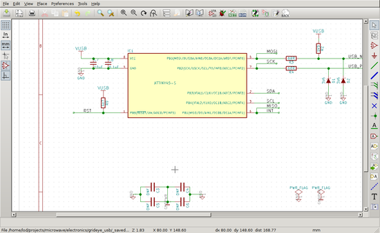
Eeschema is nice and familiar, you can place parts, connect wires, create named nets etc. I had a very simple five component board so had no need of the advanced features. However there was obvious functionality for buses and a fair bit of support for nested sheets. There is annotation tool to name your parts and a basic rule checker to catch mistakes.
Bonus
A nice bonus for Eeschema is the ability to have two names on a net. This is a bit controversial, Altium forbids it but I like it. Some times a line has two roles, such as being the MISO communication line during programming and the I2C interrupt line during normal operation. I like being able to create a named net for each role and connect both to the pin of the chip. The PCB layout program needs a single name, Eeschema handles this by arbitrarily picking one of them.
Missing Feature
Altium has a feature they call directives. This allows a pair of wires to be identified to be routed as a differential pair. You can also specify net classes, so as to specify increased track widths for the power rail or the required clearance on a high voltage track. KiCad does allow this to be done in Pcbnew but I feel the schematic, as the documentation for the design, should contain this information. This is particularly important if the layout and design are performed by different people.
Awkward
Eeschema’s use of dragging with the left mouse button is odd. In most applications this would perform a group select, in eeschema it selects and begins to move the components. Copy/paste is done by holding down shift before doing a selection. The oddness and learning curve aside, this doesn’t scale well. There is no way of selecting a group of objects so you can’t do a group delete, you can’t change the properties of a group or resize multiple wires together. Using the copy/paste you can’t double check what you have selected before doing a copy, multiple pastes require the full process to be run again and you can’t change sheets. The move is still the action regardless of the tool selected, so dragging with the wire tool actually does a select/move and placing a box like a sub-sheet must be done with two clicks not a drag.
I suspect the select behaviour will be changed in the same batch of work as the shortcut improvements. 🔗
Ugly
I should open by saying I couldn’t really get my head around the schematic libraries. My understanding is that a library file can hold multiple components but I couldn’t figure out how to put a second component into a library file. I did see notes suggesting that you merge two libraries by editing them by hand.
Several people have created their own tools to try and assist managing libraries 🔗 🔗 🔗. The existence of these tools indicates that many others have also encountered problems.
There is hidden magic behind the library process. For example to create a power component, basically a power net flag, the pin must be hidden. The pin still gets a wire connected to it but if it is not hidden it doesn’t connect to the power net and you get unconnected errors when running the rule check. This isn’t documented, the nice folks in the IRC channel explained it to me.
There is also documented hidden magic where some parts, fortunately none I used, have hidden VCC pins so they magically get the power rail without cluttering your schematic. Which is not so useful in the modern environment of multiple signal levels.
The developers are well aware of all of these issues, half the roadmap entries for eeschema are related to component editing. 🔗 The plan seems to be to migrate the backend of the schematic library to the pcb library file format and work. Then build better editing tools on top. The PCB library tool is a significant step forward.
Pcbnew
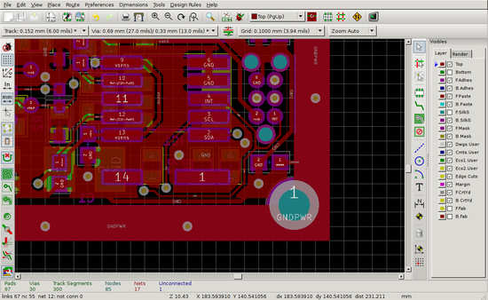
It took me a while to realise that there are actually three different PCB programs bundled into Pcbnew. They are listed in the view menu as three different display modes: default, OpenGL, and Cairo. This is not, as you might expect, just a different display engine. Some features are not available in all modes and some features work differently depending which mode you are in. I found Cairo ran very slowly on my poor ancient laptop so I just used default and OpenGL.
Differential routing is a relatively new feature and is only implemented in OpenGL. In the default view the feature on the menu is simply disabled, grayed out, no feedback is provided as to how to enable it. 🔗
There are other, lesser issues:
- In GL mode the scroll bar arrows don’t work, dragging does.
- Rubber band drag mode only works in default mode.
- In normal mode deleting a track deletes the attached via, in GL mode it does not.
- In normal mode the start track shortcut starts a track immediately, in GL mode it waits for a click.
There is a 3D model feature which uses VRML world files for each part. However it only supports the subset generated by wings3d, more complex files silently fail. Extending this to other model types is on the roadmap.
Some other stuff feels a bit incomplete:
- Hiding a copper layer still shows the pads.
- There is a “Hide all copper layers but active” option for single sided work but it doesn’t hide the other side’s silkscreen.
- The rule-check doesn’t enforce track width.
Finally the library management is better than Eescheema’s but still needs a lot of work.
- Relative paths require manually using an environment variable, which was listed in the Eeschema library manager but not Pcbnew’s.
- There is a plugin to add github based repositories, but the option is listed even if the plugin is not installed.
- There is a plugin to add github based repositories, not git based, it uses a github webpage URL.
- Adding a library doesn’t check that the library exists, works or is valid. An error is shown later when you try and use it.